STM32 Synchronous Rectification Buck-Boost Digital Power Supply
A high-performance digital power supply based on the STM32G474, featuring a four-switch Buck-Boost architecture for wide-range voltage regulation. It supports up to 450W output (48V 10A) with dual DC and USB-C PD inputs, utilizing high-resolution PWM and PID control for precise power management.
This project presents a comprehensive design for a four-switch Buck-Boost digital power supply. Built around the STM32G474 microcontroller, the system is capable of handling both step-up and step-down conversions, supporting a wide input and output range up to 48V and 10A. The design includes complete hardware schematics, PCB layouts, firmware source code, and 3D enclosure models.
Design Performance and Specifications
The power supply is engineered for high-power applications, capable of delivering a maximum output of 450W. Key parameters include:
- Input/Output Voltage: 0.5Vdc to 48Vdc (Input starts at 12Vdc).
- Maximum Current: 10A.
- Switching Frequency: 181.333 kHz.
- Voltage Ripple: Peak-to-peak ≤ 200mV.
- Efficiency: Up to 94.3% depending on load conditions.
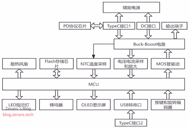
System Architecture
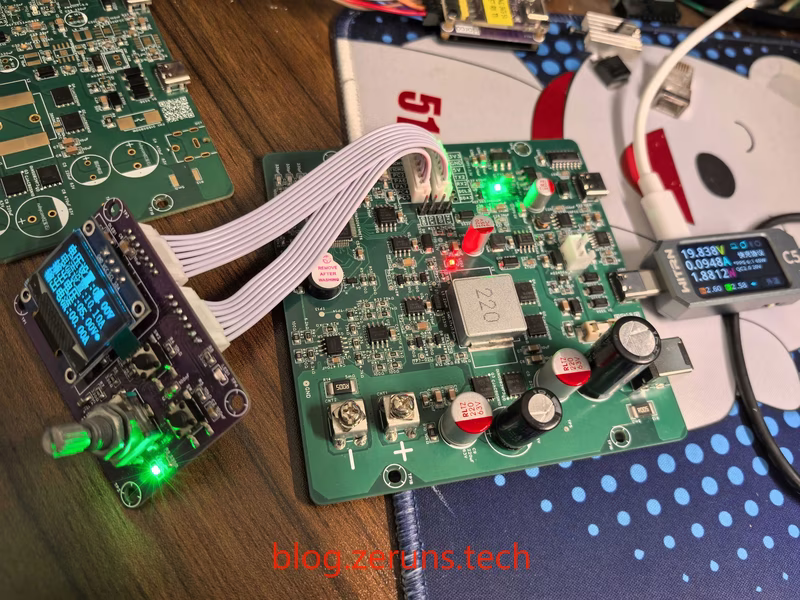
The system is divided into several functional blocks: the MOSFET drive circuit, the 4-switch Buck-Boost power stage, signal conditioning for voltage and current sensing, a PD fast-charging protocol circuit, and the MCU control unit. It features dual power inputs: a standard DC5.5 interface and a Type-C interface equipped with a CH224K protocol chip to request up to 20V from PD-compatible chargers.
Hardware Circuit Design
Power Stage and Component Selection
The core of the power conversion is a four-switch topology. Component selection was rigorously calculated to handle high currents. For the inductor, a 22μH unit with a saturation current over 10A was chosen to balance ripple requirements across both Buck and Boost modes. The output filtering uses a combination of a low-ESR 220μF solid capacitor and a 470μF electrolytic capacitor to minimize voltage ripple.
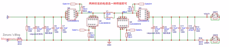
The MOSFETs selected are CJAC80SN10, which provide 100V breakdown voltage and 80A current capacity. Their low RDS(on) (6.2mΩ) and low output capacitance (Coss) are critical for maintaining high efficiency and reducing switching losses.
Driving and Auxiliary Power
Driving the high-side N-MOSFETs is handled by two EG3112 non-isolated complementary dual-channel drivers. These chips include integrated bootstrap circuits and dead-time control to prevent cross-conduction.
The auxiliary power system is a multi-stage design to ensure stable operation for the MCU and peripherals. It uses a TPS54360B to step down input voltage to 12V, followed by an SY8205 for a 6V rail, and finally linear regulators (AMS1117) to provide clean 5V and 3.3V rails. A dedicated REF3033 high-precision voltage reference is used for the MCU’s ADC to ensure measurement accuracy.
Signal Conditioning
Voltage and current sensing utilize differential amplification to reject high-frequency switching noise. Low-offset GS8558-SR operational amplifiers are employed to scale the input/output signals (up to 52.66V and 10.65A) into the 3.3V range required by the STM32’s ADC.
MCU and Software Control
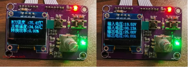
The STM32G474RET6 serves as the brain of the device. It leverages its High-Resolution Timer (HRTIM) for precise PWM generation and high-speed ADCs for real-time monitoring. The firmware implements PID algorithms to regulate output voltage and current. System parameters and safety thresholds (over-voltage, over-current, and over-temperature) are stored in an onboard W25Q64 Flash chip. Users can interact with the system via an OLED screen, a rotary encoder, and buttons, or through a PC-side host software (VOFA+) via the CH340C USB-to-Serial interface.
Testing and Validation
Performance validation shows excellent stability. In a typical 36V input to 12V 2A output scenario, the ripple peak-to-peak value was measured at approximately 42mV. Efficiency tests highlight the effectiveness of the synchronous rectification, peaking at 94.3% when converting 48V to 36V at nearly 10A.