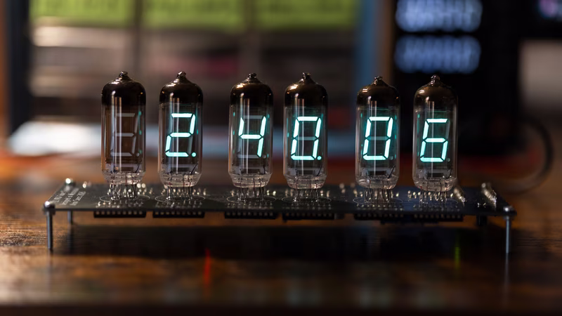
IV-11 VFD Tube Clock
A custom-built 6-digit clock utilizing Soviet-era IV-11 vacuum fluorescent display tubes and an Arduino Nano Every. The project features a static drive architecture for maximum brightness, integrated power conversion for high-voltage rails, and a robust finite state machine for user configuration and timekeeping.
Overview
The IV-11 VFD Tube Clock is a 6-digit timepiece designed around vintage Soviet-era vacuum fluorescent display (VFD) tubes manufactured in the 1970s and 80s. Unlike many modern kits, this project was designed entirely from the ground up, encompassing custom schematic design, PCB layout, and original firmware. It serves as a marriage of vintage display technology and modern microcontroller control.
Hardware Architecture
The hardware design centers on driving six IV-11 7-segment tubes in a static configuration. To achieve this without multiplexing, the design employs a dedicated 74HC595N shift register paired with a UDN2981A high-voltage source driver for every single tube. These components are daisy-chained via SPI, allowing the microcontroller to update the entire display while maintaining constant, full brightness on every segment.
Power Supply and Timekeeping
Operating from a standard 5V USB source, the clock utilizes two onboard switching converters to meet the specific voltage requirements of VFD technology:
- An XL6009 boost converter steps the 5V input up to 25V for the anode and grid rails.
- An LM2596 buck converter steps the 5V input down to 1.5V to power the tube filaments.
For precise timekeeping, the system uses a DS3231 real-time clock (RTC) module communicating over I2C. This module includes a CR2032 battery backup and offers an accuracy of ±2ppm, ensuring the clock loses less than one minute per year.
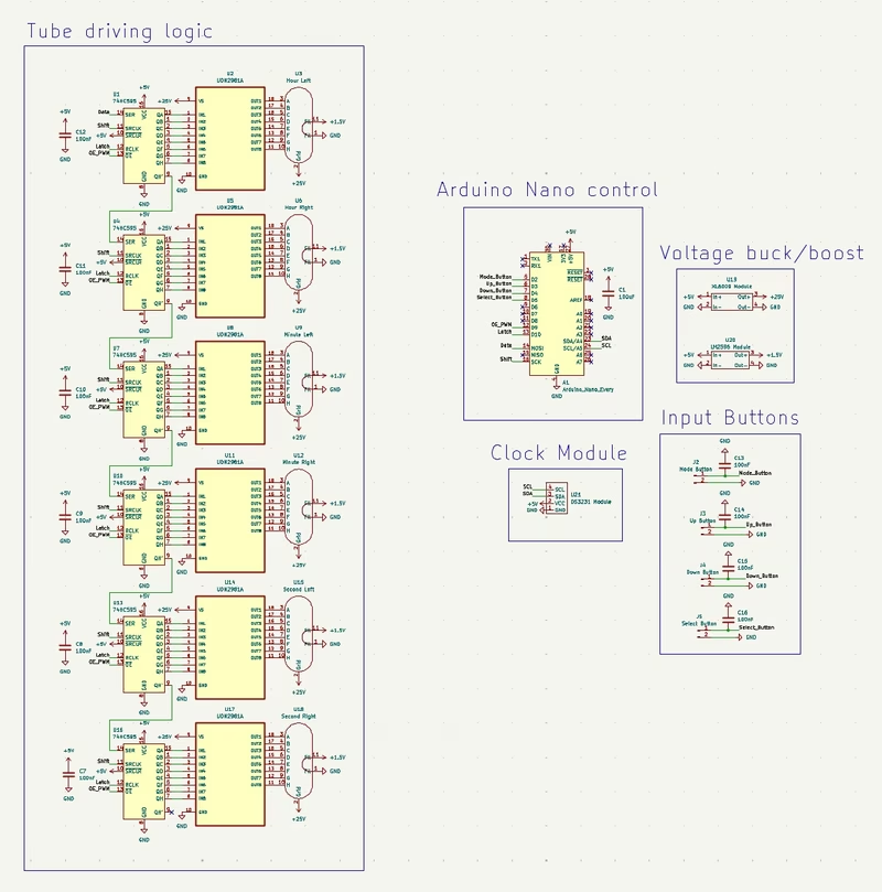
Microcontroller
An Arduino Nano Every serves as the brain of the project. It handles SPI communication for the display drivers, I2C for the RTC, and manages user input. One notable feature is the use of the shift registers’ Output Enable (OE) pin, which the Nano Every controls via PWM to provide software-adjustable brightness levels.
Firmware and User Interaction
The firmware is structured around a 7-state Finite State Machine (FSM) to manage all user interactions through a simple button interface. The FSM allows users to cycle through several modes:
- Normal clock display
- Time setting (Hours, Minutes, and Seconds)
- Manual brightness control (Levels 1–9)
- Auto-brightness toggle (Scheduled dimming based on the time of day)
- 12/24-hour format toggle
To ensure a seamless user experience, the firmware includes hardware and software debouncing for button inputs and utilizes the EEPROM to persist user settings like brightness and time format across power cycles.
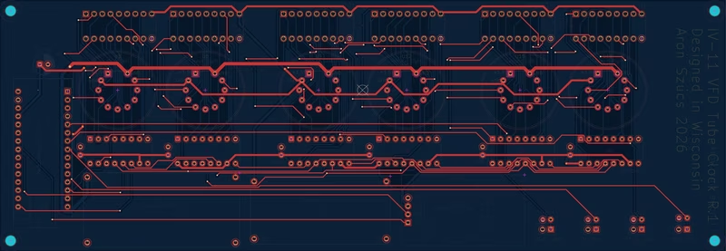
PCB Design
The project features a 2-layer PCB designed in KiCad and manufactured by JLCPCB. The layout includes custom footprints for the IV-11 tubes and the specific buck/boost modules used. Signal integrity and power delivery were prioritized by using a solid ground plane on the bottom layer and sizing power traces according to their current demands: 1.0mm for the 600mA filament rail and 0.5mm for the 25V anode rail.
Design Decisions
Several key engineering choices were made to balance complexity and performance:
- Static vs. Multiplexed Drive: A static drive architecture was chosen over multiplexing to prioritize maximum tube brightness. While this increased the component count, it simplified the firmware and resulted in a more vibrant display.
- Module Integration: Standalone pre-made buck and boost modules were used instead of discrete circuits. This reduced the complexity of the first PCB revision and allows for easy replacement if a module fails.
- Controller Choice: The Arduino Nano Every was selected over more powerful options like the ESP32. Since the project did not require wireless connectivity, the 5V logic of the Nano Every simplified the design by avoiding the additional voltage level management required by 3.3V microcontrollers.
- Signal Integrity: During prototyping, button bouncing was a significant issue. This was resolved by adding 100nF hardware debouncing capacitors to each button GPIO pin, which, combined with software logic, eliminated false presses.
Build and Implementation
The assembly process involved mapping each shift register bit to its physical tube segment using a custom-written tube tester utility. This ensured the digit lookup table in the final firmware was accurate. Despite a minor initial challenge with a mirrored tube footprint convention in the design phase, the final revision of the PCB worked flawlessly, resulting in a production-ready design.
Related Projects
EleksTube IPS Custom Firmware
This project provides a feature-rich custom firmware for ESP32-based EleksTube IPS digital clocks, enabling internet time synchronization and weather updates. It utilizes the TFT_eSPI library for high-quality display management and LittleFS for asset storage, while offering a web-based configuration portal and MQTT integration for smart home ecosystems.
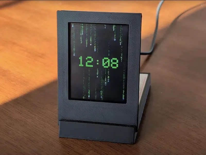
Digital Rain Clock
A Matrix-inspired desktop clock featuring animated digital rain on a 2.8-inch TFT touchscreen. Built with an Arduino Nano ESP32, the project combines real-time clock functionality with dynamic visuals, touch-based time adjustment, and customizable color schemes.