FazyRV -- A Scalable RISC-V Core
FazyRV is a minimal-area RISC-V RV32 core featuring a scalable data path that can be configured to 1, 2, 4, or 8 bits at synthesis time. It is designed for resource-constrained FPGA architectures like iCE40 and ECP5, offering fine-tuned trade-offs between hardware area and performance while maintaining compatibility with the LiteX SoC builder.
FazyRV represents a unique approach to RISC-V processor design, specifically targeting environments where silicon real estate or FPGA resource consumption is the primary constraint. Unlike standard 32-bit processors that process full words in a single cycle, FazyRV utilizes a scalable data path that allows developers to precisely navigate the trade-off between performance and area.
The Chunk-Based Architecture
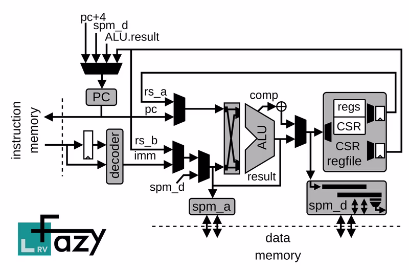
The core’s primary differentiator is the CHUNKSIZE parameter. By processing operands in smaller “chunks” of 1, 2, 4, or 8 bits, the core can drastically reduce its logic footprint. When the chunk size is set to 1, the processor operates in a bit-serial fashion; a 32-bit addition requires 32 cycles to process. While this increases the Cycles Per Instruction (CPI), it results in an incredibly small core. Scaling up to an 8-bit chunk size reduces that same operation to just 4 clock cycles, providing a significant performance boost for a relatively modest increase in area.
Design Variants and Flexibility
FazyRV is designed to be highly configurable through several parameters:
- Configuration (CONF): Users can choose between
MIN(minimal area, no interrupts),INT(basic interrupt support), andCSR(Control and Status Register support for more complex system requirements). - Register File Type (RFTYPE): The core supports multiple register implementations. While
LOGICuses LUT or FF RAM, theBRAMoptions allow the register file to be mapped to FPGA block RAM. Special bypass variants (likeBRAM_DP_BP) are available to mitigate the performance impact of sequential BRAM reads by making operands accessible one cycle earlier. - Memory Interface: The default interface is Wishbone, but a
MEMDLY1mode is available for systems with predictable single-cycle memory access (like internal BRAM), further lowering the average CPI.
Integration and Ecosystem
The project is well-integrated into the modern open-source hardware ecosystem. It features native support in the LiteX SoC builder, allowing users to instantiate a FazyRV-based system with simple command-line arguments:
litex_sim --cpu-type=fazyrv --cpu-chunksize=4 --cpu-rftype=LOGICFor standalone development, the repository includes a reference SoC (fsoc) and supports a wide range of FPGA architectures, including Lattice iCE40 and ECP5, Gowin, Xilinx, and GateMate. The build system is managed via FuseSoC, making it easy to port to different hardware targets.
Rigorous Verification
Despite its minimal size, FazyRV does not compromise on correctness. The core undergoes extensive testing and verification using several industry-standard frameworks:
- RISCOF: The RISC-V Architectural Compliance Test framework ensures the core adheres to the RISC-V specification.
- Formal Verification: The design uses
riscv-formaland SymbiYosys for formal checks of instructions and register integrity. Module-level formal checks are also applied to the ALU and data path components. - Benchmarks: Performance is tracked using the Embench suite, allowing for direct comparison with other minimal-area RISC-V cores.
Maintainable RTL Design
A notable philosophy of FazyRV is its commitment to human-readable SystemVerilog. Many minimal cores rely on manual gate-level optimizations that make the code difficult to maintain. FazyRV avoids this by writing at a standard RTL abstraction level. However, for critical sections like the instruction decoder, it uses a table-based approach that can be processed by the ESPRESSO logic optimizer. This allows the design to benefit from automated logic reduction while remaining accessible to developers who wish to modify or extend the core.