AVAJA Debug Probe
AVAJA is a compact USB debug probe designed for RISC-V softcores and FPGA development boards. Powered by the WCH CH32V307 RISC-V microcontroller, it integrates a CMSIS-DAP v2 JTAG interface, a target UART bridge, and target-powered level translation onto a single PMOD-sized board.
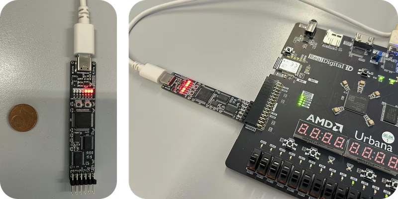
A Compact JTAG and UART Debug Probe for FPGA Development
When developing RISC-V softcores on FPGAs, having a reliable, low-latency debugging bridge can save hours of frustration. AVAJA (A Very Advanced JTAG Adapter) addresses this need in a compact PMOD form factor. By combining a CMSIS-DAP v2 JTAG transport, a high-speed target UART bridge, and automatic level shifting, AVAJA delivers an all-in-one debugging tool designed to plug directly into FPGA development boards.
At the center of AVAJA is the WCH CH32V307RCT6, a 32-bit RISC-V microcontroller clocked at 144 MHz. The probe provides native USB-C connectivity with full-speed USB support and built-in ESD protection, eliminating the need for bulky proprietary debug dongles.
Architecture and Capabilities
AVAJA is architected to handle multiple serial and debugging streams concurrently over a single USB connection:
Host PC
  |
  | USB-C / USB full speed
  v
CH32V307RCT6
  |-- CMSIS-DAP v2 ------> GPIO JTAG engine
  |-- Target UART CDC ---> USART2
  |-- Debug Log CDC
  `-- Reserved GDB CDC
          |
          v
  VREF-controlled level translators
          |
          v
     2x6 PMOD target
Multi-Interface USB Layout
Using TinyUSB on bare-metal firmware, AVAJA enumerates with multiple USB CDC and vendor-specific endpoints:
- CMSIS-DAP v2 Interface: Direct high-speed bulk endpoints (
0x07/0x87) allowing OpenOCD or other debugging hosts to control the target JTAG chain. - Target UART Bridge: A dedicated USB CDC ACM interface tied to hardware USART2, enabling seamless serial communication with running firmware on the target.
- Debug Log CDC: A secondary CDC ACM stream streaming diagnostic information and probe status back to the host.
- Reserved GDB CDC: Planned future support for an on-probe embedded GDB server, allowing host-less debugging.
Safe Voltage Level Translation
Interfacing with varied FPGA I/O banks requires careful voltage handling. AVAJA incorporates SN74LVC8T245 bus transceivers powered directly by the target’s reference rail (VREF_PMOD). The MCU monitors VREF through a high-impedance divider and keeps target-facing outputs disabled until a valid target supply is detected, preventing accidental back-powering or logic level mismatches.
Target Connector Pinout
AVAJA connects directly to target boards through a 2x6 PMOD-compatible connector (J5):
| Pin | Direction at AVAJA | Signal |
|---|---|---|
| 1, 2 | Input/reference | VREF_PMOD |
| 3, 4 | Power | GND |
| 5 | Output | JTAG TCK |
| 6 | Input/control | UART RTS / auxiliary input |
| 7 | Input | JTAG TDO |
| 8 | Output | UART RX at target |
| 9 | Output | JTAG TDI |
| 10 | Input | UART TX from target |
| 11 | Output | JTAG TMS |
| 12 | Output/control | UART CTS |
Firmware Build and Deployment
The bare-metal firmware is compiled using the riscv64-elf-gcc cross-compiler and can be flashed through either the CH32V307’s built-in USB bootloader or an external WCH-Link programmer.
# Clone submodules and compile firmware
git submodule update --init --recursive
make -C firmware

# Flash via CH32V307 USB ROM bootloader
make -C firmware flash-isp

# Or flash via WCH-Link
make -C firmware flash-wlink
Working with OpenOCD
Because AVAJA implements the standardized CMSIS-DAP v2 protocol, it functions seamlessly with OpenOCD without custom drivers. An adapter configuration script is included in the project:
openocd \
  -f firmware/openocd/avaja.cfg \
  -f path/to/your-target.cfg
The bit-banged GPIO JTAG engine supports adaptive clock frequencies ranging from 1 kHz up to 2 MHz, with hardware arbitration ensuring that CMSIS-DAP and internal debug engines cannot conflict on the bus.